US QuickTurn Prototype PCB

US QuickTurn Prototype PCB

#1 Prototype PCBs in North America

Our design rules are the least restrictive offered on quick turn prototype PCBs.

+ Smart DFM File Check - eliminate CAM holds No Extra Charge
+ Any Drill 0.008" or larger - Plated or Non Plated No Extra Charge
+ Trace Width / Spacing 0.005" / 0.005" No Extra Charge
+ Internal Cutouts - Plated or Non Plated No Extra Charge
+ Complex Board Shape No Extra Charge
+ Green Soldermask - Top and Bottom No Extra Charge
+ White Silkscreen - Top, Bottom or both No Extra Charge
+ Electrical Testing included No Extra Charge

New! FR4 Tg180 & ENIG are our new Default Specs.

Need PCB Assembly Services?
Dfm certified small

Our CAM team carefully checks your design using ViewMate with Smart DFM. We will fix minor design errors (like solder mask swell, silkscreen text size, etc.). If we find more serious errors, we will contact you about fixing your design. When you buy from us, you can be certain that your design will meet acceptable manufacturing standards.

US QuickTurn PCB Standard Specs

Material Type / Finish: FR4 Tg180 with ENIG Minimum Trace Width / Space: 0.005"
Finish Thickness: 0.062" Copper Weight: 1 oz Outer / 1 oz Inner
Soldermask Sides: Both Soldermask Color: Green
Silkscreen Sides: Top, Bottom or Both Silkscreen Color: White

Overview

US QuickTurn PCBs
Our high quality printed circuit boards are manufactured for quick-turn delivery. We offer a prototype-production quality PCB builds including green solder mask resist, Tin/Lead HASL or Immersion Silver (ROHS) finish plating, white silk screen legend, and even expedited delivery.

What are the standard PC Board features?
Available PCB Layer counts are 2, 4, 6 and 8 layers.

0.062" Thick
Minimum line and space = 0.005"
Minimum finished drill size = 0.008"
Green SolderMask both sides.
White SilkScreen Top, Bottom or Both
Tin/Lead HASL or ENIG (Immersion Gold) finish plating
Electrical test included
Irregular board shape is OK
Internal cutouts are OK

What Add-Ons are available for the US Quickturn Service?
To keep our cost low for our customers, our online service does not allow add-ons.
Please submit your files with a Request for Custom Quote

What is the standard shipping schedule for 2 layer PCBs?
For orders received by Noon PST the following business day is Day 1.

Shipping schedule for 1 Business Day orders:
Orders received by Noon Monday will ship Tuesday.
Orders received by Noon Tuesday will ship Wednesday.
Orders received by Noon Wednesday will ship Thursday.
Orders received by Noon Thursday will ship Friday.
Orders received by Noon Friday will ship Monday.

Shipping schedule for 2 Business Days orders:
Orders received by Noon Monday will ship Wednesday.
Orders received by Noon Tuesday will ship Thursday.
Orders received by Noon Wednesday will ship Friday.
Orders received by Noon Thursday will ship Monday.
Orders received by Noon Friday will ship Tuesday.

What is the shipping schedule for 4, 6 and 8 layer PCBs?
For orders received by Noon PST the following business day is Day 1.

Shipping schedule for 3 Business Days orders:
Orders received by Noon Monday will ship Thursday.
Orders received by Noon Tuesday will ship Friday.
Orders received by Noon Wednesday will ship Monday.
Orders received by Noon Thursday will ship Tuesday.
Orders received by Noon Friday will ship Wednesday.

Shipping schedule for 4 Business Days orders:
Orders received by Noon Monday will ship Friday.
Orders received by Noon Tuesday will ship Monday.
Orders received by Noon Wednesday will ship Tuesday.
Orders received by Noon Thursday will ship Wednesday.
Orders received by Noon Friday will ship Thursday.

Shipping schedule for 5 Business Days orders:
Orders received by Noon Monday will ship Monday.
Orders received by Noon Tuesday will ship Tuesday.
Orders received by Noon Wednesday will ship Wednesday.
Orders received by Noon Thursday will ship Thursday.
Orders received by Noon Friday will ship Friday.

Please keep in mind, add 1 lead-time process day for major US Holidays.
Major US Holidays do not count as a Business Day.

What are the US Quickturn PCBs prices?
Standard prices are based on square inch size of your PC board and board layer count (2, 4, 6 and 8 layers).
We will accept your files and Request for Custom Quote for anything you are not sure about.

What types of payments do you accept?
Payment terms are by credit card transactions through US Quickturn PCBs website only. We accept Visa, MasterCard, and American Express.
Bank card transactions are processed electronically through US Quickturn PCBs secure SSL web site.

If you have more questions, please contact our Technical Experts at support@pentalogix.com

Specs

What is the US QuickTurn PCB manufacturing policy?

1. Orders are not guaranteed to be accepted by us until your files pass our Smart DFM review.

2. We prefer that you pass your design through Smart DFM. This way, you can correct any errors that you find. At the end of the Smart DFM process, you can save a .ezq file. If there are no errors, then we can manufacture your board directly from the .ezq file. If you get stuck in the middle of the Smart DFM process, you can save and submit your .ezq file to us for additional help.

3. While we prefer that you send us a file after passing it through Smart DFM, you can also choose to send us your raw Gerber and Drill files. We will process your files using Smart DFM and send you an email with a detailed result of the Smart DFM checks. If possible, we will edit your files to remove any Smart DFM violations. Our email to you will detail any changes that we've made and we will send a revised .ezq file that you can load into any of our ViewMate family of products. You can review all of the suggested changes that we've made. If you're happy with our changes, then you can ask us to produce your PCB using the supplied .ezq file. However, we recommend that you change your design in your CAD system so that it passes our Smart DFM checks without requiring any alterations.

4. All files will be retained for 3 months.

5. Orders can be shipped anywhere in the world that is served by UPS or FedEx, so long as no US Export restrictions are in force.

6. We reserve the right to change prices and delivery terms at any time.

If your design contains non-plated holes
Smart DFM places plated and non-plated holes on separate layers. If you run your design through Smart DFM, please remember to check the "Non-Plated Through Holes" check box.

If you send us raw Gerber and Drill files, and your design contains both plated and non-plated holes, then we prefer that you place these holes on separate layers. This will ensure that we understand your intent. If you are using ViewMate Deluxe or ViewMate Pro, then you can also submit your data as a .bin file. Name your plated drill layer "PlatedDrills" and your non-plated drill layer "NonPlatedDrills".

Board Outlines
Your board outline does not have to be square or rectangular. You can submit round boards or boards with a complex shape. Our requirement is that we can convert your outline to a continuous unbroken path. By default, we will rout your board outline with a 0.0625" diameter rout bit. This will result in a minimum radius of approximately 0.032" on inside corners. If your design contains inside corners with radii of less than 0.032", then we will use a 0.03125" diameter rout tool to cut out your board. In this case, inside corners will have a minimum radius of 0.016".

Routing
Default rout tool diameter is 0.0625". 
All features are cut out using this tool if possible (both internal features and the board outline). 

Internal Cutouts
Your design can have both plated and non-plated internal cutouts. We suggest that you add one layer for each type of cutout (plated or non-plated). Just place elements in these layers that are the exact shape of the cutout that you want. For example, if you want a 0.050" x 1.00" slot cutout of the board, then just add a trace of this size to the appropriate layer. If you have a more complex shape, then just submit it as one or more polygons that describe the edge of the cutout. We suggest you draw the polygon with an "F-Type" shape (a line of zero width). If you choose, you can draw the polygons with any width trace. We assume that the centerline of the trace describes the edge of your internal cutout. Plated cutouts will have the inside of the cutout plated with the finish that you choose (Tin/Lead HASL or Immersion Silver (ROHS)). Non-plated cutouts will not have any plating on the internal edges. Name your plated cutouts layer "PlatedInternalRouts". Name your non-plated internal routs "NonPlatedInternalRouts". If you wish, you can also supply a drawing that details the internal cutouts and we will create the needed geometry for you. We prefer to use a 0.0625" rout bit for internal cutouts, although we will use a 0.03125" diameter bit if your design contains features with internal radii of less than 0.032".

Solder Mask Swell and "Minimum Web"
When manufacturing your board, there may be a small misregistration between the solder mask layers and the underlying copper layers. As a result, we recommend that you swell your solder mask layer so that it is 0.005" (0.0025" on a side) larger than the underlying copper elements. This way, if there is a misregistration, then your copper pads will not have any solder mask on them. You should also ensure that your design has a "Minimum Web" of at least 0.003" between adjacent pads. Smart DFM can pinpoint any problem areas for you.

Silk Screen Feature Size
We recommend that your silk screen features have a width of at least 0.007", although the absolute minimum for clear legibility is 0.005". If you submit a Smart DFM file with features that are less than 0.005", then we will simply submit your design for manufacture. There is no guarantee that these narrow features will reproduce correctly. If you submit Gerber data or a .bin file to us, then we will modify your silk screen layers if any features are less than 0.007". If possible, we will set all features so that the minimum trace width is 0.007". Where this is impractical, we will reduce the silk screen feature size to a minimum of 0.005".

Do PC Boards UL marking?
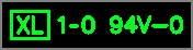
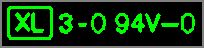
By default we add a UL marking to the bottom copper layer.
If there is no room on the bottom copper layer we add a UL marking to the bottom silkscreen.

2 Layer UL marking:

Quickturn layer1 or Quickturn layer2

Multi Layer UL marking:

Quickturn layer3 or Quickturn layer4

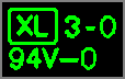
We add a Date Code, a 3 digit order fragment and a Serial Number to the bottom silk screen layer:

Quickturn layer5

Layer Stack-Up

US QuickTurn PCB Stack-Up

  2 Layer 4 Layer 6 Layer 8 Layer  
Layer 1 0.0017" 0.0017" 0.0017" 0.0017" 1.0 oz Copper
  0.059" 0.0075" 0.008" 0.0065"  
Layer 2 0.0017" 0.0014" 0.0014" 0.0014" 1.0 oz Copper
    0.040" 0.014" 0.008"  
Layer 3   0.0014" 0.0014" 0.0014" 1.0 oz Copper
    0.0075" 0.008" 0.0065"  
Layer 4   0.0017" 0.0014" 0.0014" 1.0 oz Copper
      0.014" 0.008"  
Layer 5     0.0014" 0.0014" 1.0 oz Copper
      0.008" 0.0065"  
Layer 6     0.0017" 0.0014" 1.0 oz Copper
        0.008"  
Layer 7       0.0014" 1.0 oz Copper
        0.0065"  
Layer 8       0.0017" 1.0 oz Copper
Overall Thickness 0.0624" 0.0612" 0.0610" 0.0618"  
Copper Thickness Core Thickness Prepreg Thickness

What is the minimum trace width allowed?
The minimum traces width is 0.005" (5 mils).

What is the minimum spacing between traces to copper lands?
The minimum gap between traces and copper lands is 0.005" (5 mils).

What is the minimum annular ring on vias?
The minimum annular ring on vias is 0.006" (6 mils). each side of the hole. The pad must be large enough to tent over the hole otherwise you may lose the metal in the hole during outer layer etching resulting in plating voids.

What is the closest copper to edge of board?
The closest copper trace and land fills to edge of PC board is 0.010" (10 mils). If the copper runs closer to the edge it may be exposed during board rout.

Are the boards electrically tested?
All multi-layer (4, 6, 8 and 10 layer) boards come electrically tested as part of the service. Two-layer boards are not tested.

Can you handle controlled impedance requirements?
No. This feature is not available through the US Quickturn PCBs service. However, you may submit a Custom_RFQ for complete PC board manufacturing needs.

To what acceptability standards do you build?
PCBs are built to IPC-A-6011/6012 latest revision Class 2 with inspection based on IPC-A-600 latest revision.

What files do you need to manufacture my US Quickturn PCBs?
The following files need to be compressed into one ZIP file and uploaded through the US Quickturn PCBs web site at order placement. Our web application will only accept one ZIP file per order. Your file set needs to be complete with the following data:
1. Gerber files in 274X or 274D formats. (274D format will require an aperture list or environment file)
2. Excellon2 NC drill file.
3. Drill tool list specifying finished hole sizes, hole quantities, and plated/non-plated holes.

How do I send my files?
You will be prompted to upload your files through the web site during order placement. Your files are encrypted and maintained in our secure database.

If you have more questions, please contact our Technical Experts at support@pentalogix.com

Specials

Get 20% off any Laser Cut SMT Stencil and Solder Paste when you order your PCBs!
Just place your PCBs in your shopping cart, the smt stencil and the solder paste are automatically discounted.