PCB Navigator
Transforms static Gerber files into an interactive, searchable environment by integrating BOM and XY placement data for faster inspection, troubleshooting, and documentation.
PCB Navigator gives users a faster way to work with PCB manufacturing data.
Instead of switching between Gerber files, BOM spreadsheets, XY placement files, and assembly drawings, users can view component information directly on the board layout.
This makes it easier to find parts, confirm placement, review assembly details, investigate issues, and create clear documentation for engineering, purchasing, production, and quality teams.
Key Capabilities and Use Cases
PCB Navigator is built for a wide range of users across the electronics supply chain, including PCB designers, fabricators, assemblers, and component brokers. With PCB Navigator, users can:
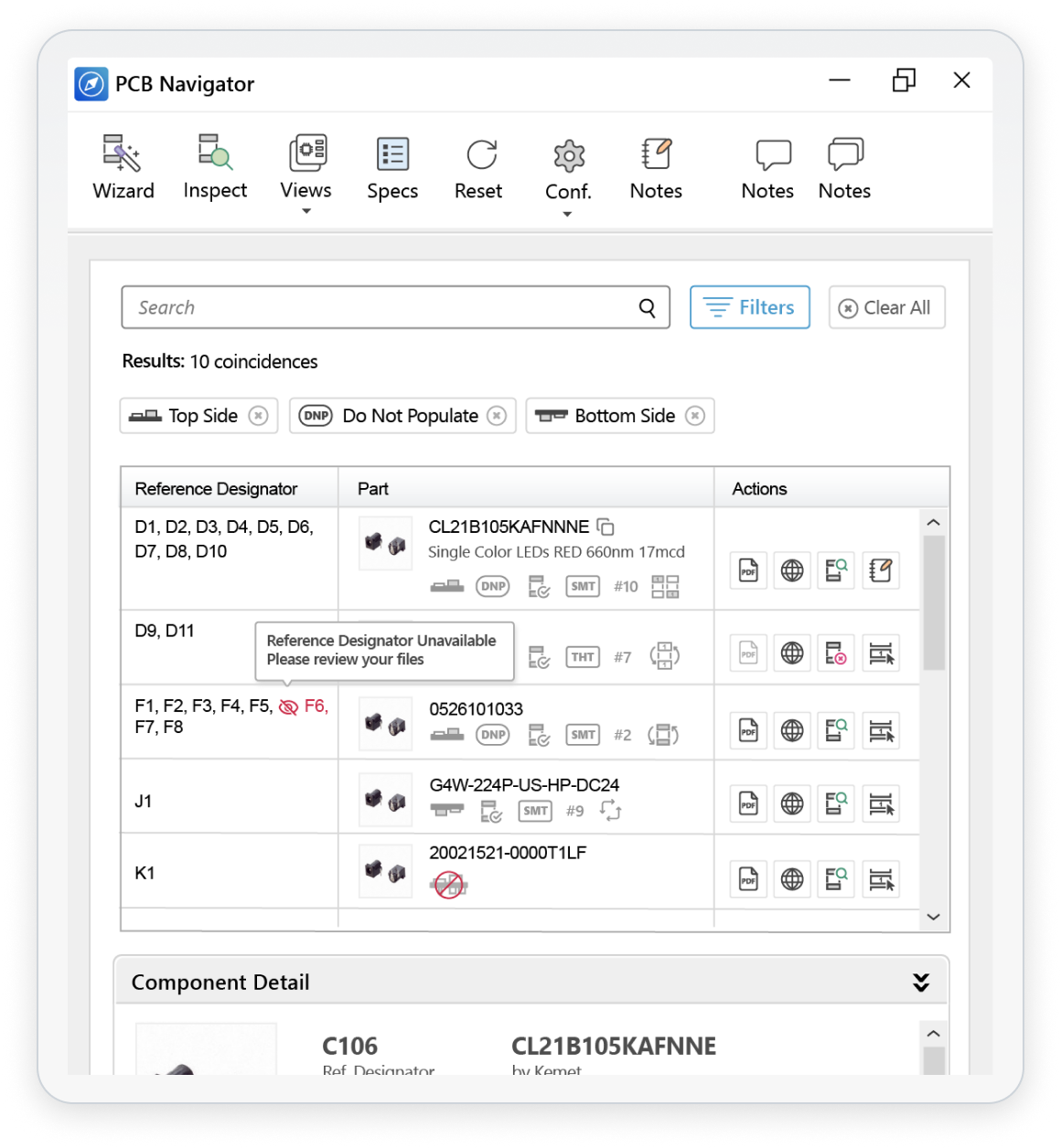
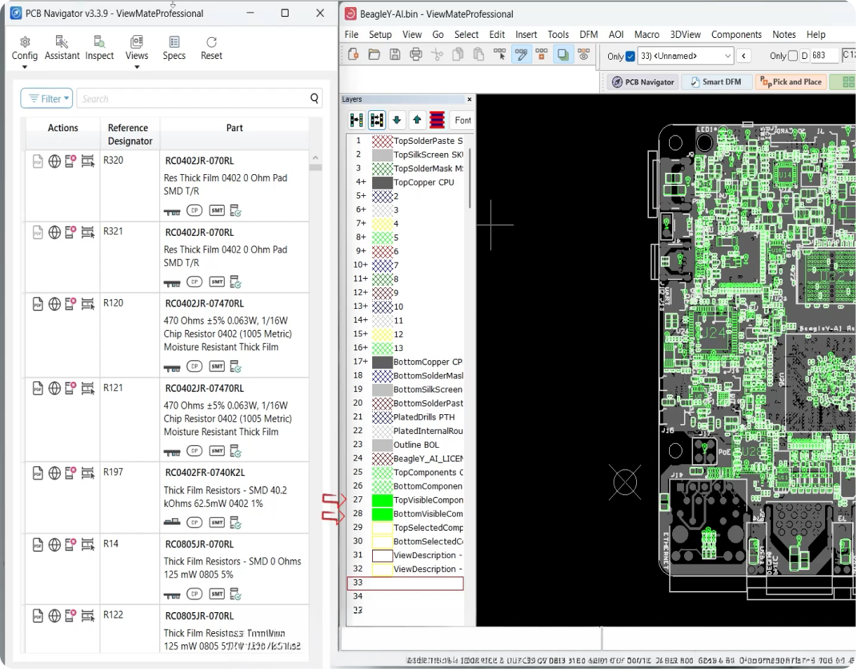
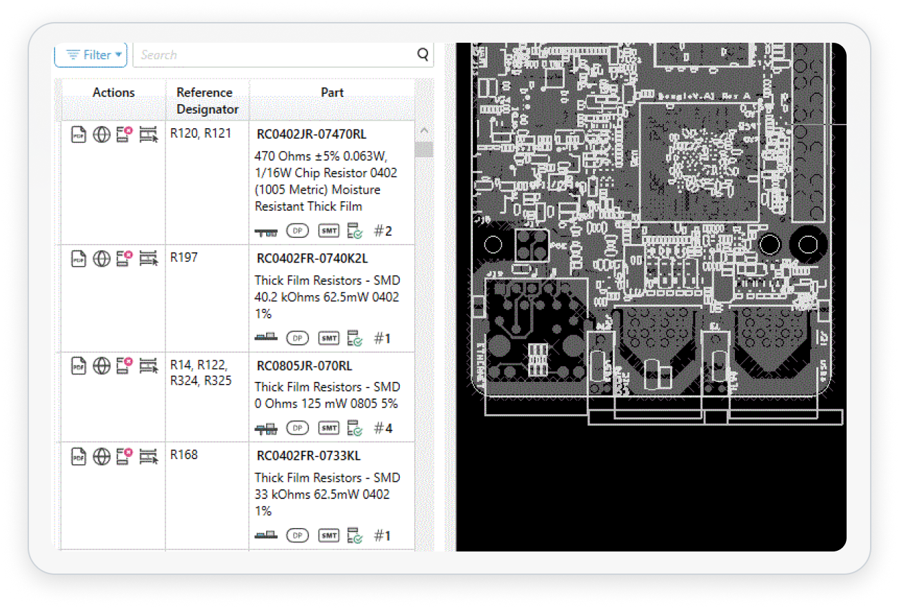
Quickly find components by reference designator, part number, or component type using the Component View. Selected components are automatically highlighted in the Gerber View for easy identification on the PCB.
Seamlessly correlate part numbers, footprints, package types, and XY placement coordinates on a single screen.
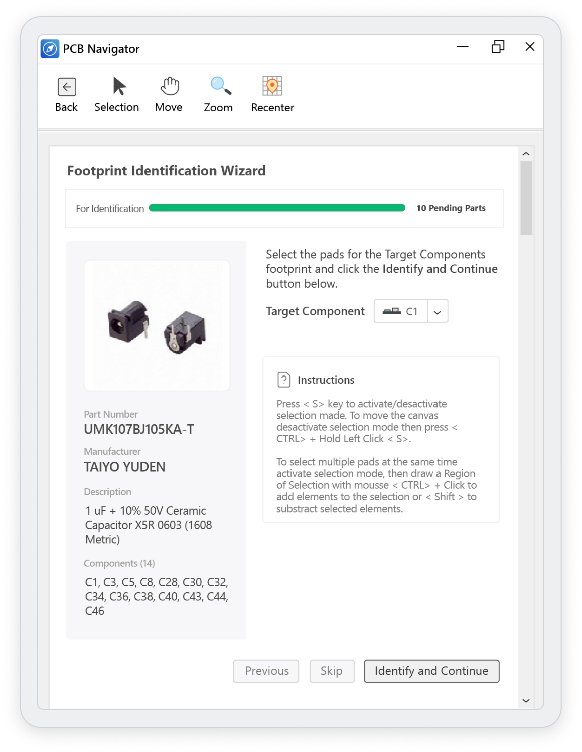
Verify component type, orientation, and board-side placement before fabrication or assembly begins.
PCB Navigator provides an excellent visual reference for discussing issues, clarifications, and design changes with internal teams and external partners.
Filters and Views
PCB Navigator includes powerful filtering and viewing tools that help users quickly focus on specific components, placement attributes, and board regions.
Key filtering and viewing features include:
Easily Filter components by board side to simplify inspection and assembly review.
Display only surface-mount or through-hole components to verify assembly methods and manufacturing requirements.
Selected components or groups are highlighted in the Gerber View while non-selected board elements are dimmed, improving visibility and simplifying inspection.
These tools simplify the analysis of complex PCB designs, help identify potential issues early in the process, and allow users to tailor the display for design review, fabrication, assembly, and sourcing activities.