Smart DFM
More than just a DFM checker, it adds intelligence to your PCB design workflow
For more information, please email us at support@pentalogix.com
What is Design for Manufacturing or DFM?
Design for Manufacturing (DFM) is a process applied before the manufacturing stage that integrates production constraints and capabilities. The goal is to make the manufacturing process easier, faster, and more cost-effective while maintaining quality and reliability.
In electronics and PCB assembly, DFM typically refers to:
- Ensuring component footprints and spacing meet assembly and manufacturing tolerances.
- Designing for efficient soldering (wave, reflow, selective solder).
- Reducing unnecessary complexity that increases cost or risk.
- Checking for fabrication limits (trace width, drill size, copper-to-edge clearance, etc.).
- Improving testability and serviceability.
Why PentaLogix's Smart DFM?
Smart DFM is part of the ViewMate toolset. It's more than just a Design for Manufacturing (DFM) checker, it adds intelligence to your PCB design workflow by helping you verify manufacturing readiness before sending files to fabrication.
Relying only on a manufacturer's in-house checks can be risky. That's why it's important to use an independent, third-party DFM tool: it gives you confidence that your files are truly production-ready, no matter where you build your boards.
With Smart DFM, you're not limited to generic checks as you can define specific rules that match your manufacturer's requirements, such as trace widths, drill clearances, or silkscreen spacing. These rule sets can be saved, reused, and shared across projects, giving you flexibility and consistency throughout your design cycle.
Some of its capabilities include:
- Early detection of potential fabrication problems (missing files, drill misalignment, malformed board outlines)
- Automated rule checks (trace widths, spacing, annular rings, copper-to-edge clearance, etc.)
- Customizable rules so you can match manufacturer requirements or your own internal standards.

How to Run Smart DFM
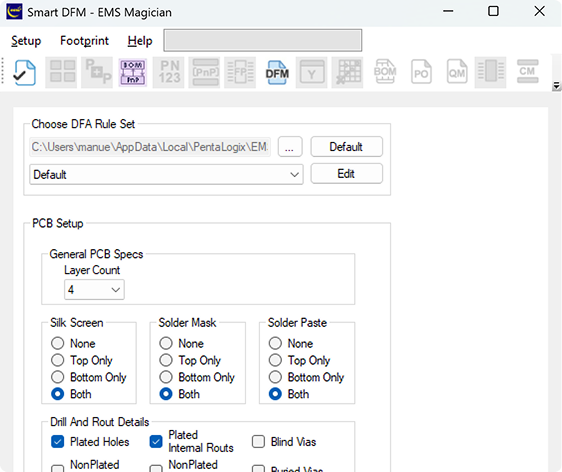
Begin by selecting the basic parameters of your design. Choose the layer count, indicate whether silkscreen, soldermask, and paste mask are present on the top and bottom layers, and provide drill and rout details. This includes checking options such as plated/non-plated holes, plated/non-plated internal routs, and whether blind or buried vias are used.
Specify the drill stackup to ensure that all hole types and via structures are properly understood before analysis.
Assign the correct layer types for your PCB design. This can be done manually, or you can use the Auto Identify feature, which automatically maps layers if their types were previously defined in the project.
Confirm the polarity (positive or negative) of each layer. Proper polarity assignment ensures that Smart DFM interprets copper and non-copper areas correctly.
Smart DFM checks that the board outline is a single, continuous, unbroken path. This step prevents outline errors that can cause manufacturing delays or misinterpretations.
All design elements outside the board outline are automatically clipped. This guarantees that only features within the valid outline are included in the DFM analysis.
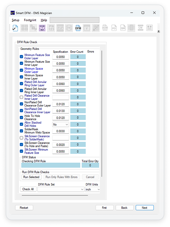
With the setup complete, you can now perform a full DFM analysis. Smart DFM evaluates your design against rule sets. Choose between either the built-in defaults or your own custom specifications to detect potential manufacturing issues before they become costly problems.

Rules
 1. Minimum Feature Size
It's the smallest conductive element (such as a trace, pad, or copper area) that can be reliably fabricated on a PCB. This rule defines the lower limit of what your manufacturer's etching process can produce without risk of breaking or under-etching. It ensures that fine copper features are not lost or damaged during imaging and etching.
For example, if a PCB manufacturer specifies a minimum feature size of 4 mil, then any trace, copper island, or plane detail smaller than 4 mils wide may not reproduce properly.
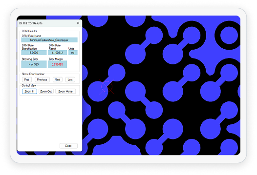
- If the minimum feature size is too small, copper may over-etch or break, leading to open circuits or poor yield.
- Manufacturers typically define this limit based on their process capability and copper thickness (e.g., 3-5 mil for standard production, smaller for HDI).
- Designers should always confirm this rule with their PCB fabricator before layout finalization.
2. Minimum Space Clearance
It refers to the smallest allowable gap between two adjacent conductive features, such as trace-to-trace, pad-to-pad, or copper-to-copper spacing.
It ensures electrical isolation between conductors and prevents shorts during fabrication, plating, or soldering.
For instance, if the minimum spacing is set to 4 mils, any distance smaller than 4 mils between copper elements may result in bridging or unwanted connections.
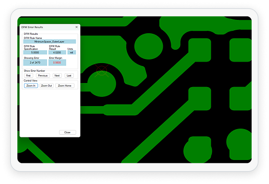
- If space clearance is too small, etching residues or solder bridges can cause short circuits.
- IPC-2221 specifies different clearance requirements based on working voltage and environment.
- Always align this rule with both fabrication and assembly tolerances to ensure long-term reliability
3. Plated Drill Annular Ring
It's a printed circuit board (PCB) design specification that refers to the smallest width of copper pad that extends beyond the edge of a drilled hole (via or component lead hole).
In other words, it's the minimum amount of copper "ring" surrounding the drilled hole that ensures a reliable electrical and mechanical connection.
The annular ring is defined as the Pad Diameter minus the Drill Diameter divided by 2. For example if a pad is 20 mils in diameter and the finished hole is 12 mils, the annular ring = (20 - 12) ÷ 2 = 4 mil.
- If the annular ring is too small, drilling tolerances can cause the hole to "break out" of the pad, leading to poor solder joints or open circuits.
- IPC standards (e.g., IPC-2221) provide guidelines for acceptable minimum annular ring dimensions, depending on whether the hole is plated through, non-plated, or via type.

The minimum width of copper pad around a plated through-hole (PTH). A proper annular ring ensures mechanical strength and reliable electrical connection between the pad and the hole plating.
4. Plated Drill Clearance
The minimum distance between the edge of a plated hole (such as vias or through-holes) and any adjacent copper feature not connected to it.
This spacing prevents unintended electrical connections or shorts caused by drill wander or plating expansion. For example, if the plated drill clearance is 8 mils, any isolated copper around the hole should be at least 8 mils away from the drill edge.
If this clearance is too tight, drill misalignment can break into nearby copper, causing opens or shorts.
Typical minimum values range from 6-10 mils depending on board thickness and layer count.
5. Non-Plated Drill Clearance
Measures the required clearance between a non-plated mechanical hole (used for tooling or mounting) and surrounding copper.
Since non-plated holes lack insulating plating, any copper too close to the drill path can expose or short the copper to hardware or the board edge.
Standard non-plated hole clearance values are often 10-15 mils, but can vary depending on manufacturer and drill tolerances.
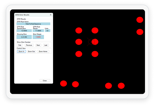
6. Hole-to-Hole Clearance
This rule specifies the minimum distance between the edges of two adjacent holes.
If holes are too close, drill hits can merge or weaken the board structurally. Some manufacturers allow this for specific cases like large oblong openings, but it's generally not recommended due to potential tool wear, poor plating, or irregular edges.
7. Allow Stacked Drill Holes
This rule determines whether overlapping or stacked drill hits are permitted.
This practice is typically discouraged because stacked holes can cause registration issues, tool breakage, or poor plating quality. The rule's purpose is to prevent potential fabrication errors and ensure drill data integrity.
8. Soldermask Minimum Web / Space
This rule defines the smallest strip ("web") of soldermask that can exist between two exposed copper areas.
If the soldermask web is too thin, it can peel, chip, or fail during assembly. For example, if a fabricator specifies a 4-mil minimum soldermask web, there should be at least that much distance between adjacent soldermask openings.
A narrow mask web may not adhere properly or could cause shorts during reflow. Common minimums range from 3-5 mil for standard processes, and this rule is critical for fine-pitch components like BGAs.

9. Silkscreen Clearance
This clearance defines the minimum spacing required between silkscreen text or graphics and functional features such as pads, holes, and soldermask openings.
This rule ensures that silkscreen ink does not overlap solderable or exposed areas, which could cause contamination during soldering.
For example, if a silkscreen-to-pad clearance of 5 mil is set, Smart DFM will flag any reference designator or marking printed closer than 5 mils to an exposed copper feature.
10. Silkscreen Minimum Feature Size
It refers to the smallest printable line width or text height that can be clearly reproduced by the silkscreen printing process.
It ensures legible reference designators, logos, and markings after fabrication.


