EDA tools like Altium Designer, PADS, OrCAD, and many others provide design engineers with extremely powerful and intelligent capabilities to create complex schematics and to design intricate PCB layouts. But when it comes to transitioning from design to manufacturing, the process of preparing accurate and optimized manufacturing files can be complex and error-prone. Taking a set of Gerber files and sending it off to a fabricator without much verification presents a great opportunity for a wide variety of manufacturing errors that are easily preventable. While fabricators may or may not catch some of these errors on their own, this potential break in communication and data integrity is something that PCB designers can actively address by creating a much more holistic approach to their designs. This is where dedicated PCB CAM tools come into play, since they are offering significant advantages in streamlining manufacturing data preparation. For PCB designers, integrating a CAM tool into the workflow can transform the accuracy and reliability of the handoff to manufacturers and significantly increase the efficiency of the process.
How CAM Tools Streamline Manufacturing Data Preparation of PCBs?
CAM tools are specifically designed to handle the intricacies and intelligently manage the complexity of PCB manufacturing data. They provide a dedicated environment for processing, validating, and optimizing the output files generated by PCB layout software. In this function, CAM tools are a core element of an effective Design for Manufacturing or DFM process. And the fact that they operate independently from the EDA system is especially important when it comes to enhancing manufacturing data preparation in the following areas:
Validation and Error Checking
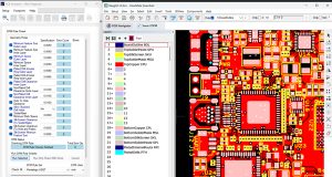
One of the core features of CAM tools is their ability to independently validate manufacturing data before it is sent to the fabricator. They perform rigorous checks to ensure the files are complete, correctly formatted, and free of issues that could disrupt production. For instance, a CAM tool can verify that all layers align properly, drill holes match the design, and apertures are correctly defined in Gerber files. Such a validation is critical because even minor discrepancies can result in defective boards. This can include issues such as misaligned drill files or incorrectly assigned Gerber layers. CAM tools also include Design Rule Checks or DRCs that are specific to manufacturing, and that go beyond the electrical DRCs in most EDA tools. These checks flag issues like insufficient solder mask coverage, overlapping drill holes, or violations of minimum trace widths or minimum spacing that can cause a board to be entirely unmanufacturable. Using a comprehensive DRC in a CAM tool based on the actual manufacturing data is allowing designers to identify and address any of these issues before the files are even sent to production.
Customization for Manufacturer Specifications
Every PCB manufacturer has its own set of requirements, which are a function of the specific manufacturing technology employed by the fabricator as well as their individual manufacturing processes. These specs range from preferred file formats and file naming conventions to specific tolerances for characteristics such as trace widths, spacing, or board outlines and keep-out zones. Modern CAM tools allow designers to create and save custom profiles for different manufacturers, ensuring that all output files are tailored to the fabricator’s specifications. This eliminates the need to reconfigure settings for each project or for each different fabricator, which is substantially streamlining the preparation process.
The Impact on the PCB Design Workflow
Integrating an independent CAM tool into the PCB design workflow delivers significant advantages. Automation and validation save time by streamlining the preparation and troubleshooting of manufacturing files, freeing designers to focus on innovation. By detecting errors early and optimizing manufacturing files, state-of-the-art CAM tools minimize the risk of expensive rework or scrapped boards, which significantly reduces both overall cost and time-to-market. An efficient relationship between designer and fabricator incorporates a significant amount of tribal knowledge on both ends, and standard export Gerber files from most CAD systems don’t necessarily have the depth of information that is required for an effective handoff. Standardized, manufacturer-ready files enhance collaboration by creating a robust communication interface between PCB designers and both PCB fabrication as well as PCB assembly, by minimizing delays and misunderstandings. Validated manufacturing data also ensures the final PCB aligns with the design intent, which enhances product quality and reliability. For complex designs, high-volume production, or projects with multiple manufacturers, a CAM tool is essential. It bridges the gap between design and production, ensuring that the transition is smooth, efficient, and error-free.
In today’s world of advanced PCB design, where precision and efficiency are paramount, CAM tools play a pivotal role in streamlining manufacturing data preparation. By validating manufacturing files, customizing files for specific manufacturers, and supporting fabrication-specific specifications for advanced manufacturing processes, these tools enhance the reliability and efficiency of the design-to-production pipeline. For PCB designers, integrating a CAM tool into their workflow can be a strategic decision that saves time, reduces costs, and ensures high-quality outcomes. As PCB designs continue to grow in complexity, the role of CAM tools in achieving manufacturing success will only continue to get more critical.


