DFM Accountability is the Foundation of Modern PCB Success
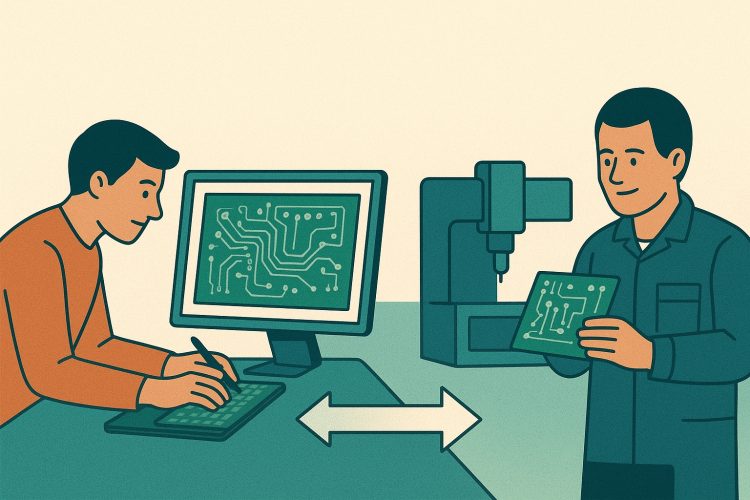
The electronics industry is in a constant race to bring products to market at a breakneck pace and the pressure on printed circuit board fabricators these days is enormous. Modern CAD systems like Altium Designer, KiCad, or Eagle empower engineers with evermore intelligent tools to create extremely complex layouts with great precision, but the transition from digital design to manufacturing a physical circuit board is too often a rough road with lots of hidden perils. The output files like Gerber and Excellon NC drill format are the universal industry language between designer and fabricator, but these file formats while universally accepted by pretty much everyone in the industry, are extremely rudimentary and allow for many potential manufacturing problems to go completely undetected by the CAD system operator. Using CAM software for the manufacturing files is not a luxury nowadays, but pretty much a necessity. CAM software transforms the sometimes quite chaotic handoffs into a streamlined, and very much predictable workflow, which ultimately allows design teams to meet today’s challenging production timelines that are most often measure in days than weeks, rather than having to deal with sometimes significant delays that could be entirely preventable. These tools are validating, correcting, and optimizing manufacturing files before they ever reach the fabricator.
Gerber files digitally represent every layer of a PCB, the copper traces, solder mask, silkscreen, and board outline, as a series of vector commands using various apertures. Whereas drill files define the exact coordinates, diameters, and plating requirements for every drill hole. These files are generated automatically from the CAD system, but the focus of most CAD systems is on electrical connectivity, signal integrity, and component placement, while manufacturing feasibility is unfortunately often only an afterthought. Just because a set of production file exports without error from the CAD system does not mean that it won’t quickly become problematic when it is scrutinized even for basic fabrication specs such as a minimum trace and space by the fabrication team.
One of the most common issues is layer misalignment. Even a small offset between the top copper layer and the solder mask can cause exposed traces or partially blocked pads, which can be highly problematic during assembly. In multilayer boards, any unintended offset of inner layers can lead to catastrophic failures such as shorts or open connections when vias fail to align with their intended landing pads. Silkscreen and solder mask files are also very frequent culprits of manufacturing errors. If silkscreen layers are printed over pads or holes, then there is a high probability of it causing inconsistent or open solder joints, and a silkscreen layer that is designed too narrow will most likely not print at all, since there is a minimum resolution threshold for the screen-printing process that is used to apply silk screen to PCB. Many CAD systems apply a default offset or pull-back for solder mask layers, to prevent that the solder mask being printed onto the pad, but with higher density components, such standard offset parameters can be too large, unintentionally resulting in no solder mask being printed between some solder pads, which can lead to printing errors and even to shorts on the finished boards.
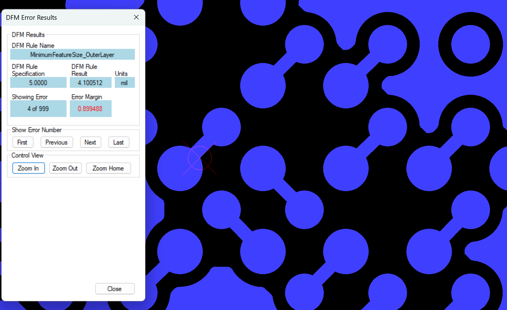
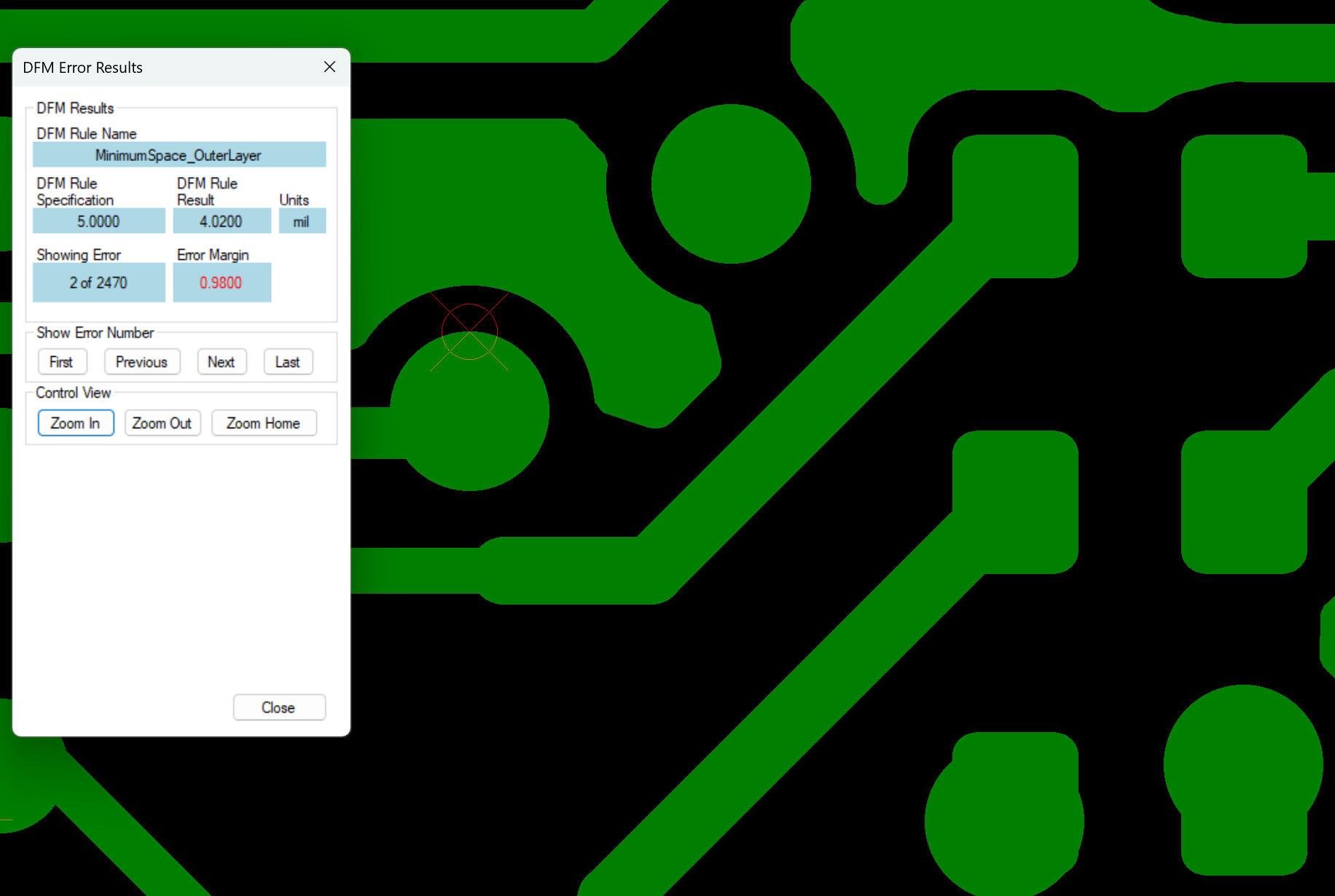
However, these fabrication issues are certainly not limited to the Gerber files. Drill data is also often the cause of manufacturing errors. Drill holes may overlap with traces or pads, or the annular rest ring of the via pads is too small for a reliable connection. For instance, a rest ring of 3 mil might look fine on the CAD screen, but such tight tolerances could be extremely tough to produce in real life. And in some cases, plated drill holes and non-plated drill holes are exported in the same drill file with no clear distinction between the two, which can cause a real mess in fabrication. Another common issue is that some drill hole diameters used in the design are much too small to be reliably plated unless you are using a very high-end board shop. HDI designs can even amplify these risks. Blind and buried vias with high aspect ratios (e.g. exceeding 3:1) are quite challenging to plate uniformly by most board shops and can therefore result in voids or weak connections.
Incomplete files, set-up, or missing data can compound these problems even more. For example, a missing board outline leaves the fabricator guessing what the overall dimensions of the board might be, especially if a dedicated routing file is not provided. And even when files are complete, data corruption during export or use of obsolete file formats can introduce ghost apertures or misinterpreted vector data, leading to features that exist in the file but not in the intended design. Fabrication drawings are another critical component in the CAD-to-fab transfer process. Such files typically contain important notes on impedance control, surface finish, or material stack-up that are critical for the manufacturing process. Omitting such fabrication drawings from the set of manufacturing files generated by the CAD system, leaves this area wide open to guesswork or a lengthy back-and-forth communication between the design and fabrication teams. Poorly named layers (e.g. TopCopper, L2, Bottom, etc.) without clear stack-up order is another issue that is fairly common. They might require the fabrication team to manually interpret the data, burning hours of engineering time and still potentially ending up in a bit of a coin toss.
These are just a few examples of how manufacturing files that are generated from CAD systems can unexpectedly result in completely unintended consequences. Unfortunately, these are not rare oversights. In fact, industry data suggests that 30 to 40 percent of first-time PCB submissions in CAD-to-fab handoff contain at least one critical error that would halt production or cause scrapped boards if not caught early. Operating an independent CAM software tool prior to handing off manufacturing files to the fabricator might prove its worth for the PCB designer. It only works off the native fabrication files and simulates the entire manufacturing process. CAD systems prioritize electrical rules and often overlook manufacturing nuances or ignore specifications that can vary from fabricator to fabricator. However, CAM systems typically have very advanced DFM capabilities, helping to align layers, verify drill-to-copper clearances, validate aperture lists, and check solder mask expansion against pad geometry. They also detect annular ring violations, ensure that minimum trace widths comply with the fabricator’s process capabilities, and flag non-functional pads, orphaned copper fragments, along with a number of other manufacturing-related aspects.
Just simply pressing the export button in a CAD system and sending the generated data set off to fabrication without a thorough DFM process and “hope for the best” is simply not a viable option in today’s fast-paced environment. The expectations for quick turnaround, ever-faster time-to-market, and lowest possible manufacturing cost are simply too great to ignore. The possibility of manufacturing errors with unverified manufacturing files is enormous, amplified by the fact that standard Gerber and NC-Drill files on their own, while accepted pretty much everywhere, simply don’t provide a great enough built-in level of intelligence to be used without thorough independent validation and additional manufacturing information.


