
In the fast-paced world of PCB design, time is everything. You’ve spent weeks perfecting your schematic, routing traces, and ensuring signal integrity. Finally, you generate those Gerber files and send them off to your preferred PCB fabricator. It’s a moment of relief: the design is out of your hands, and production can begin. But what happens next? In the printed circuit board industry, this handoff is notoriously known as “throwing it over the wall”, which is a term that vividly captures the abrupt, one-way transfer of files with minimal communication between designers and fabricators. And behind that wall lies a host of unknowns that could torpedo your production timeline, or worse, undermine your design’s performance.
The “wall” isn’t just a metaphor; it has in fact become a literal barrier erected by the hyper-competitive nature of global PCB fabrication. With razor-thin margins and instant online quoting systems, fabricators prioritize speed and customer retention above all else. They battle for volume in a market dominated by low-cost providers, with many of them being overseas, where a single delay could send a client jumping ship to a competitor. As a result, when your unverified production files arrive, which could potentially contain issues such as undersized drills, misaligned layers, or missing board outlines, fabricators often choose not to object. Instead, they might quietly intervene, or they might not. The uncertainty is the real problem, and it leaves designers in the dark, perpetuating a cycle of inefficiency and missed opportunities to improve.
The Competitive Blind Spot: Silent Fixes and Their Consequences
Imagine submitting a set of Gerber files with a subtle flaw: a solder mask opening that’s too narrow, risking shorts during assembly. In an ideal world, the fabricator would flag it, explain the issue, and request a revision. This feedback would allow you to refine your design process, perhaps by adjusting your CAD tool settings or incorporating better tolerances. But in reality, many fabricators opt for silence in favor of speed. Their in-house engineers might resize the opening, shift a layer, or add the missing outline without necessarily consulting the designer. The boards arrive on time, function (mostly), and you can move on to the next project. While such a “fix-and-forget” approach system keeps the production line moving, it comes at a steep hidden cost to you, the designer.
First, there’s the unpredictability: Fabricators may or may not fix your errors. Some issues, like minor drill size discrepancies, are easy to correct in-house. Others, such as impedance mismatches or poor panelization, might slip through if they’re deemed non-critical to the fabricator or if the production engineer is rushed. What if the fix introduces a new problem? A shifted layer could inadvertently create EMI issues in your high-speed design, leading to failures in the field that you might attribute to assembly rather than the silent alteration during board fabrication. Without communication, you’ll never know. This Russian roulette with your files erodes trust in the supply chain and exposes your projects to unnecessary risks.
More critically, the lack of communication stifles you and your team’s professional growth. Every uncaught error reinforces bad habits. Maybe you’ve been routing traces too tightly, ignoring fabrication tolerances, or skipping basic Design for Manufacturing (DFM) checks in your CAD software. Over time, these oversights become ingrained. You might produce functional boards, but they’re far from optimal and could be wasting materials, reducing yields, and potentially increasing costs downstream. Industry data shows yield rates hovering at 85-90% when 98%+ is possible with proper DFM. That gap represents scrapped panels, excess material use, and environmental waste, all because the feedback loop is either broken or not in place at all.
Without dialogue across the “wall,” designers and fabricators operate in silos. You might not realize that your stack-up lacks embedded impedance data, or that your panelization could be optimized for better efficiency, potentially cutting costs by 10–20% or more depending on volume and optimization. This forces the fabricators to make assumptions, and they often take on these burdens to keep customers happy. However, they rarely share their insights. The question is, why? Providing detailed reports could reveal trade secrets or slow down the PCB fabricators’ workflow. In rare instances, designers might receive a generic email about a “minor adjustment”, but obtaining any substantial advice on enhancing their DFM process is extremely uncommon, if not nonexistent. Unfortunately, this built-in opacity prevents the entire industry from evolving, and it is slowing innovation in areas where precision is paramount to reach maximum performance.
The Real-World Impact on Designers
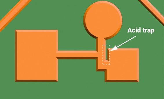
As a PCB designer, you’re on the forefront of electronics innovation. Whether you’re crafting boards for IoT devices, medical equipment, aerospace, communications, or automotive systems, your work demands reliability and efficiency. Yet, by “throwing it over the wall” with unverified files, you gamble on the outcome, betting that the fabricator will catch whatever potential DFM violations your CAD may have missed. CAD tools are powerful for layout and simulation, but they’re not infallible. They frequently overlook fabrication-specific pitfalls such as annular ring violations, acid trap formations, or silkscreen overlaps that could lead to production issues. DFM rules can also vary from company to company since they are based on the fabricator’s experience, process flow, and also their technical capabilities.
The consequences extend beyond individual projects. Repeatedly submitting flawed files without correction leads to stagnant skills. You miss out on learning best practices, such as adhering to IPC standards. Over time, this could make you less competitive in the job market, where more employers value designers who prioritize DFM from the outset. Moreover, in high-stakes fields, undetected issues could lead to significant delays, product recalls, safety hazards, or even financial losses, all scenarios where the design phase can quickly become an object of heightened scrutiny.
Breaking the Cycle
While “the wall” stifles communication, you don’t have to wait for fabricators to tear it down. The solution lies in integrating independent CAM tools into the workflow, like Gerber viewers or Gerber editors. These aren’t just add-ons to a CAD system; these tools are essential for detecting issues that CAD overlooks, which is why it is so important that they are independent of the CAD. Working with the same data that the fabricator sees allows you to prevent manufacturing errors and, more importantly, learn and improve your design process and foster a robust DFM culture.
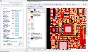
Professional Gerber Viewers and Gerber Editors allow you to validate your Gerber files before submission. They run comprehensive checks for drill tolerances, layer alignments, solder mask clearances, and more, generating detailed reports that highlight warnings in plain language. This catches errors early, reducing revisions and accelerating time-to-market.
Beyond detection, CAM empowers self-improvement. By reviewing reports, you learn to anticipate fabrication challenges, like optimizing trace widths for better yields or embedding stack-up data to eliminate ambiguity. Some advanced CAM platforms even simulate panelization, helping you minimize waste and costs. With standards like ODB++ or IPC-2581 gaining traction, CAM facilitates seamless data exchange, turning your files into a blueprint for success rather than a puzzle for the fab.
Incorporating CAM isn’t complicated. It can start with a simple Gerber Viewer that integrates with the CAD environment to validate the production files. Beyond that, a more powerful Gerber Editor can run validations after layout completion, addressing issues, and generating a DFM report to accompany your submission. Over time, CAM should be treated as a core review step, akin to schematic simulations. Training resources, online forums, and industry certifications can help designers master it quickly.
Building a Better Design Culture
Printed circuit board designers must recognize the perils of “throwing it over the wall.” The existing culture of silent fixes, or no fixes at all, denies PCB designers the insights needed to refine their workflows and elevate their DFM practices. Hoping for valuable input from across the wall is in most cases a losing strategy. It only perpetuates errors, wastes resources, and hampers innovation. Instead of waiting for the fabricator to speak up, the design team should empower itself with the right tools and transform uncertainty into precision. Independent Gerber Viewers and Gerber Editors are an indispensable part of the process. By detecting errors before they become “production issues” these tools help to produce cleaner designs, foster better yields, and build a culture of continuous improvement.


