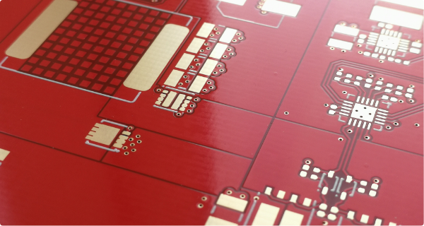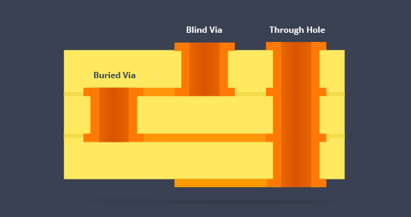
A via (also known as vertical interconnect access) is a copper plated hole that allows electrical connection between layers of a printed circuit board. The hole can be made using a drill or laser. A via consists of a barrel, a pad, and an anti-pad.
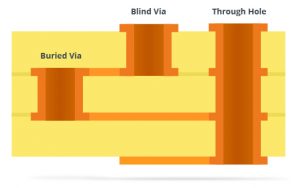
Through-Hole Vias
A through-hole via is a copper plated hole that traverses the entire printed circuit board from one top to bottom. It forms a conductive path that connects all the layers. Through-hole vias are the easiest and most cost effective to fabricate.
Blind Vias
A blind via is a copper plated hole that connects the top or bottom layer of the printed circuit board to one or more of the inner layers. Unlike through-hole vias, blind vias do not go through the entire board thus they are only visible from one of the outer layers.
Buried Vias
A buried via is a copper plated hole that connects two or more of the inner layers of a printed circuit board. Buried vias do not go through the entire board and they are not visible from any of the outer layers.
Pros and Cons of Using of Thrugh-hole, Blind and Buried Vias
Blind and buried vias are used to free up space when the PCB is small and space is limited. They are mostly used in high density interconnect (HDI) printed circuit boards. Buried vías free up surface space on the top and/or bottom side of the board for traces and SMT components. Blind vías free up inner layer space. Through-hole vías on the other hand, waste space on all the inner layers that they traverse to make their connections.
The disadvantage of blind and buried vias is that they add additional steps to the manufacturing of the PCBs increasing the cost significantly.