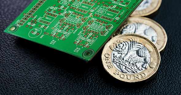
In the world of circuit board prototyping, it is a known fact that copper is used as an interface between the actual board and the components. However, if the copper is not properly installed, there can be many problems that could eventually cause the PCB to become unusable. As a way to prevent this, laminates and finishes often come into play.
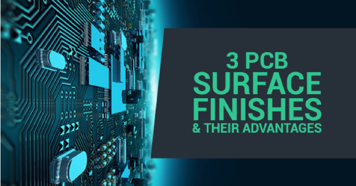
Generally speaking, laminates are manufactured by curing under pressure with temperature layers of cloth or paper. The paper has a thermoset resin to form an integral final piece of uniform thickness, with the maximum size between four to eight feet in width and length. But these days, there is much more information available concerning prototype printed circuit board finishes. Here, we explain some advantages that come with each.
Immersion Tin
This is a metallic finish that is deposited by a chemical displacement reaction. Applied directly on top of the copper on each board, this tin prevents oxidation and prolongs the board’s life.
The advantages of using this method include:
- Tin and copper adhere to each other exceptionally well
- It creates a flat surface
- You can rework it again and again until it fits correctly
- Ideal if you are using the Press Fit Pin Insertion method
HASL and Lead-Free HASL
As the most popular choice in the industry, this process is relatively easy. It requires the engineer to place the board directly in molten tin or lead alloy and then remove the unneeded solder by blowing hot air across the board.
The advantages of using this method include:
- Cost-effective
- Better observation of delamination issues before the PCB fabrication is completed
- Easily accessible
- Durable and long-lasting
OSP and Entek
Organic Solderability Preservative is a finish that prevents the prototype PCB’s finish from oxidizing. By applying a thin layer over any copper, this method will protect the copper before the soldering takes place.
The advantages of using this method include:
- Quite a simple process to complete, great for beginners
- Affordable, as the process can be applied to the prototype PCB over and over again
- Creates a flat surface
Don’t know where to start when it comes to choosing the right laminate for your PCBs? Give our professionals a call today!