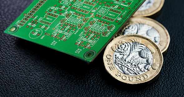
Circuit board prototyping is a complex science, and there are so many components that need to go onto one board. There are a variety of soldering techniques one can use to attach these components to the printed circuit board including high volume production and bulk wave soldering.
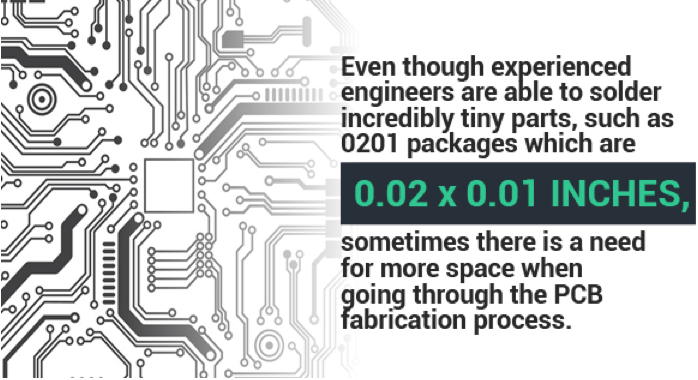
Typically, high volume production is completed with an SMT placement machine and bulk wave soldering utilizes reflow ovens. Even though experienced engineers are able to solder incredibly tiny parts, such as 0201 packages which are 0.02 inches by 0.01 inches, sometimes there is a need for more space when going through the PCB fabrication process. This is where blind and buried vias can come in.
What is a blind and buried via?
Simply put, these are connections within the board that connects components to each other on different layers.
A blind via is a copper plated hole that connects one outside layer to multiple inner layers. These vias never go all the way through the board and are created with a separate drill file than traditional vias.
A buried via on the other hand, connects two outside layers to one or more inner layer. You are unable to see these vias as they are literally buried within the outer surfaces of the prototype pcbs.
The benefits of using these vias:
There are many advantages of using these techniques when manufacturing a board. They include;
- Gives the engineer the ability to fit multiple components on a very small surface.
- Drilling these vias doesn’t impact any traces or other surface mount components on both the top and bottom of the board.
- One is able to place the SMD pad over the buried via, allowing for a better aesthetic look and more variety when it comes to placing components.
- A great way to increase test coverage
- Allows for the same digital and net pin diagnostics.
These blind and buried vias bring quite the advantage to any and all printed circuit boards. If you are interested in learning more about how this technology can benefit your specific projects, do not hesitate to contact our experts at Pentalogix today.