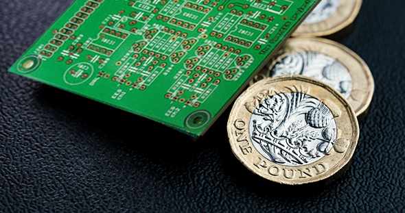
It is no secret that in today’s world, our technology is getting smaller and smaller. This especially goes for prototype printed circuit boards, which are the backbone of many electronics on the market, from your cell phone to your television and everything in between.
But in the world of PCB assembly, smaller prototype circuit boards are not always a good thing. Space is a rarity on the boards, as engineers need ample room to place all the necessary components. On a typical printed circuit board prototype, FR-4 glass epoxy is the primary insulating substrate, with a laminated thin layer of copper foil on either side. This is where the components are placed, but for those who need to save space on the FR-4 substrate, this is where blind and buried vias can come in.
Here is a brief intro guide into this technique in circuit board prototyping.
What is a via?
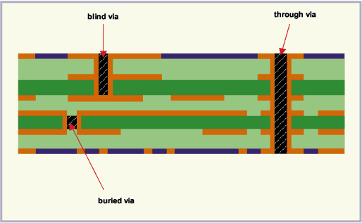
Simply put, a via is an electrical connection between two different layers of a circuit. These connections are electrically connected through holes in the board and this is where the terms blind and buried come from.
What is a blind via?
A blind via is a hole that is only connected to one surface on the board, even though they occur on two different layers. They’re most often used for SMT pads, as they must be accessible to physical probes.
Their advantage: the ability to widen the board’s breakout channel and reduce layer count.
What is a buried via?
A buried via is completely buried within the board, and cannot be seen even if the board is picked up and looked through. They are used to connect components that are not external.
Additional advantages: these holes do not take up space on the surface of the board, and they hold the ability to trade the SMD pad placement.
Are there any disadvantages of having blind or buried vias?
Yes, only with buried vias. Because they don’t have access to the outside of the board, they do not have access to external probes and cannot be put through standard circuit tests.
Utilizing blind and buried vias is one of the best ways to make a PCB design as efficient as possible. If you are interested in learning more about this interesting technique and how it can help you enhance your prototype circuit board, call us today.