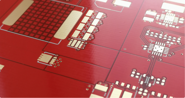
An important part of the PCB design process is creating the footprints. Tiny mistakes during this stage may result in a failed design, no matter how clean and perfect your layout is.
And the bad news is that is very easy to make mistakes during footprint creation if you don’t pay enough attention to what you are doing. That’s why you must include some degree of verification process to your workflow. This will not guarantee a zero-error rate, but it will reduce the probability of mistakes considerably.
Take your time to understand the part’s datasheet and mechanical drawings
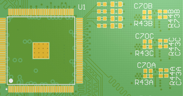
Before jumping into the footprint editor and start adding pads, silkscreen and any other object, spend a few minutes understanding all the information provided by the datasheet. For example, check if the drawing is a top or bottom view, so you know if you have to mirror the footprint or not. Try to identify all the key information in advance, such as pitch, pads’ length and width, or if there is a thermal pad or not.
Always verify pin numbers
This may sound obvious, but many designers skip this stage, which is one of the most common causes of wrong footprints. A good advice is to put both the datasheet and footprint editor windows side to side and double check that all pins are in the correct order.
If possible, have a colleague check your footprint
If you are working with a team of PCB engineers, it is nice to mutually verify other’s work. It’s a win-win situation. It doesn’t have to be a very extensive check, sometimes a quick look from another pair of eyes may catch problems that you didn’t see.
3D models or STEP files can save your day
Adding a 3D model to your PCB footprint is strongly recommended. Not only will make your final designs look nicer and more professional, but it will help you verify and detect issues the geometry of the footprint. Pitch mismatches, pads having the wrong dimensions or locations, or verifying placement of additional elements such as polarity / pin-1 markings are all things that can be easily detected by placing the 3D model on your footprint and inspecting it in 3D mode. Nowadays most CAD packages have built-in 3D visualization, and most parts manufacturers let you download their component’s 3D models for free, so there’s no excuse!