Gerber Standards
If you are involved in the electronic industry and particular with Printed Circuit Boards (PCBs), chances are that you have heard the terms “Gerber” or “Gerber files”. But what do they mean exactly?
The files that you submit to a PCB manufacturing house are in a vector format called Gerber. This format was developed by UCAMCO in the early eighties for the purpose of standardizing the data used in the production of Printed Circuit Boards. Since then, it has evolved to overcome multiple issues and adapt to the modern times. Drill layers are usually in NC formats, but it is common practice in the industry to use the term “Gerber files” to refer to any set that contains data in Gerber and/or NC drill formats.
Despite the fact that all Gerber files follow the same standards, each CAD software has its own variations in the way files are exported. Moreover, users can add an extra layer of differentiation during the file generation process depending on how they configure the exporting process, resulting in different conventions that sometimes lead to issues when manufacturers attempt to interpret the data. Let’s discuss some of the most common sources of confusion when dealing with Gerber files for PCB manufacturing.
Filenames and Extensions
During the export process, each printed circuit board layer (Top/Bottom/Inner copper, solder mask, silkscreen, board outline, etc.) is converted into a separate Gerber file. Unfortunately, there is not a standard convention for naming the various PCB layers. The most common PCB design software available in the market follow one of these two approaches: either adding a suffix to the filenames, or adding a file extension for each layer exported. For example, files generated with Altium Designer and Eagle use the second approach, while KiCAD follows the first. Some CAD packages allow the user to customize the filename and extensions of the Gerber output, but on some others these parameters are fixed. Things can get confusing when there are multiple conventions.
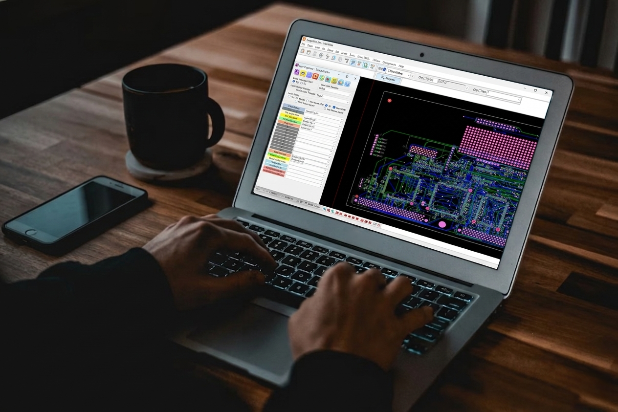
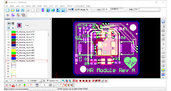
Printed circuit board manufacturers process hundreds or thousands of orders every week, they can (in most cases) identify board data correctly, but there are some cases when ambiguity forces them to be put an order on hold until further clarification from the customer. At PentaLogix, we recommend to use explicit filenames as identifier for each PCB layer. Our CAM software can do this with just a few clicks thanks to the Layer Organizer tool in ViewMate and CAMMaster.
| Board Layer | Naming/extension convention | |||
| Altium | Eagle | KiCAD | Pentalogix recommendation | |
| Top Copper | Filename.GTL | Filename.cmp | Filename-F_Cu.gbr | TopCopper |
| Bottom Copper | Filename.GBL | Filename.sol | Filename-B_CU.gbr | BottomCopper |
| Top Silkscreen | Filename.GTO | Filename.plc | Filename-F_SilkS | TopSilkscreen |
| Bottom Sillkscreen | Filename.GBO | Filename.pls | Filename-B_SilkS | BottomSilkscreen |
| Top Soldermask | Filename.GTS | Filename.stc | Filename-F_Mask.gbr | TopSoldermask |
| Bottom Soldermask | Filename.GBS | Filename.sts | Filename-B_Mask.gbr | BottomSoldermask |
| Board Outline | Filename.GM1 | Filename.mil | Filename-Edge_Cuts | BoardOutline |
| Plated Drills | Filename-Plated.TXT | Filename.drd | Filename.drl | PlatedDrills |
| NonPlated Drills | Filaname-NonPlated.TXT | Filename.drd | Filename.drl | NonPlatedDrills |
Table 1. Typical Gerber Naming/Extension Conventions
Units: Metric vs Imperial
Most PCB CAD software tools allow to choose between metric or imperial (or English) units. Using either of them is completely Okay, however, it is always recommended to avoid mixing them up. Export all your files in metric or imperial units, but never a mixture of both, as this can cause problems during production.
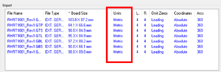
Figure 1. Using uniform units for all Gerber files being imported
Controversial layers
Some layers can be considered “special” and often bring controversy between engineers when deciding which is the correct way to export them as Gerber files. Among these layers we can include the board outline and the drill layers.
Many PCB designers export the board outline embedded into another layer file (top or bottom copper, silkscreen, etc.). This can be confusing to the manufacturer, as it may not be clear whether the outline primitives belong to the outline or if they are part of the copper, silkscreen or the layer being shared with the board outline elements. That’s why we recommend to export the board outline as a separate, stand-alone Gerber file containing a continuous, unbroken path defining the board edges.
Another source of debate is the separation of plated or non-plated holes. We recommend to separate plated and non-plated drills into different files in order to avoid any kind of confusion. Most PCB design software tools enable this option.
Final words: Avoiding CAM holds depends on your best practices
Every time your order is put on hold you waste time and money, so a little extra effort to assure this won’t happen before sending the files to the printed circuit board manufacturer is greatly valuable. Following best practices when generating Gerber data is a lesson that many engineers have learned the hard way. We want you to learn it the easy way by following these simple tips!