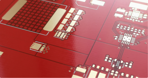
Printed Circuit Board assembly using automated equipment such as pick & place machines, stencil printers and reflow ovens provides higher efficiency than manual methods. It is a great option for prototype pcb assembly and low volume production, and the only viable option for high volume production. But automated PCB assembly imposes certain requirements that need to be met when designing and manufacturing a printed circuit board. An important part of these requirements is related to the PCB panel. In this article we will discuss what a panel is and how to avoid the most common problems related to the panelization of PCBs.
What is a PCB panel?
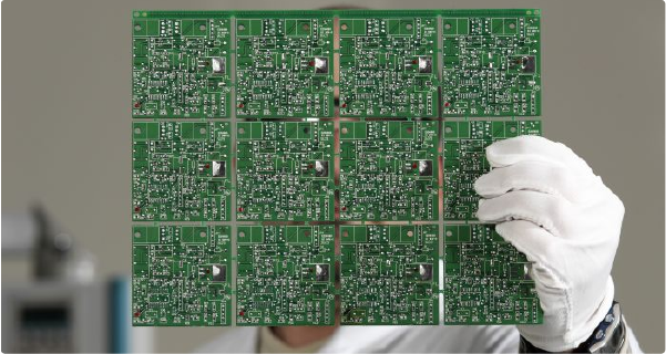
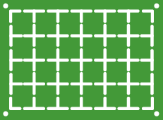
A PCB panel is an array of multiple individual printed circuit boards connected together to form a single, larger board. The most common case is to have panels with multiple copies of the same design, but in occasions different board designs can be combined into a single panel. The process of creating panels is called PCB panelization.
When to use PCB Panels?
If you are hand-soldering enthusiast, you may not need to panelize your printed circuit boards. But if you plan to contract a PCB assembly shop, chances are that you will need to panelize them. Some of the most common reasons why PCB assembly houses will require you to panelize your PCBs are:
- Boards are small. Automated equipment has limitations in terms of the minimum board size they can handle. If the individual design is very tiny, this problem can be solved by creating a larger panel with appropriate dimensions
- Quantity is high. By combining multiple printed circuit boards into a single panel, you increase efficiency as a larger number of boards can be processed at the same time. Hence, PCB panelization helps you save time and money, especially when dealing with large production volumes.
- Components are too close to the edges. Since panels have rails, PCB panelization is a safer way to process boards than individual PCB assembly. We’ll talk about rails later in this article.
How to depanelize?
Panels are a great technique for optimizing PCB assembly, but the final printed circuit boards need to be separated after the assembly is finished. In order to depanelize the PCBs in a safe manner, two alternatives exist:
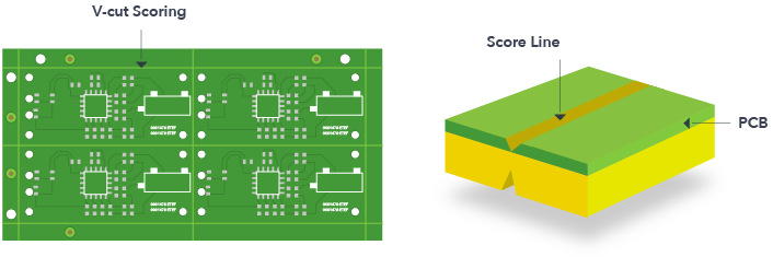
V-scoring
This method consists of straight-line V-shaped groves created between the individual printed circuit boards on both sides of the panel (top and bottom). These groves remove about two thirds of the board material, leaving a thin section that is strong enough to keep the panel together, but easy to cut away using a tool cutter blade (similar to a pizza cutter) once the assembly is done.
This option saves cost compared to other methods because no spacing is required between individual boards, reducing the overall panel size. Because the V-grooves must be straight lines, it is a great option for square or rectangular boards, but it does not work with circular or some complex geometries. It can also lead to problems when components overhang the board edge as they may be damaged by the cutter tool. In those cases, it is recommended to use the next method.
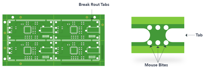
Tab-routing
Instead of the V-shaped groves, this method works by cutting slots (routs) between the printed circuit boards, connecting them with short perforated tabs (commonly named “mouse-bites). These tabs can be broken away after the assembly to separate the boards.
Because the routs are created using CNC machinery, this method has the advantage of working with any board shape. It also works well when boards have overhanging components, as long as no tabs are located right under those elements. The downside lies in that the routes require some spacing between individual boards (typically 0.1 – 0.2 in) increasing the overall panel size (and hence fabrication cost).
What are Rails?
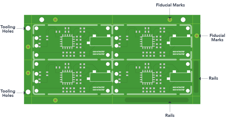
One of the main purposes of panelization is safe handling of the PCBs during assembly. Rails play a big role on this.
Rails are frames made of the same PCB material enclosing the array. They provide support and structural integrity to the panel but also allow conveyor belts and SMT equipment to grab and transport the panel safely, avoiding damage to the electronic components placed on the printed circuit boards.
The key aspects to look at when adding rails to a PCB panel are width, tooling holes and fiducial marks:
- Rail width: It is important to add sufficient width to provide adequate strength to the panel. However, the wider the rails, the more board area required, hence increasing the fabrication cost
- Tooling holes: Always add three or four non-plated holes for tooling. A diameter of around 0.12 inches is suitable for most cases
- Fiducial marks: Adding at least two fiducial marks (plated pads free of solder paste) is recommended so the pick and place machine vision system can use them as a geometric reference.
Who can panelize my printed circuit boards?
When ordering PCBs, you can submit your files in single format or panelized. If you send single board files, most PCB manufacturers can panelize your design at no extra cost.
Feel free to send us your Gerber files at support@pentalogix.com. We are happy to help with all your PCB needs, including PCB panelization and guidelines to ensure that your boards are ready for assembly. If you need more information about panelization, simply email us or give us a call at (800) 208-1726.