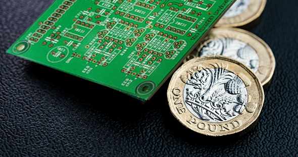
When creating a prototype circuit board, the PCB layout is one of the most important aspects. The layout is exceptionally important considering if the smallest of things goes wrong, the entire board will be compromised and it will not function properly. One of the most important steps in the prototype PCB assembly process is the imaging process, which helps to create the circuit pattern.
Laser direct imaging (LDI) can help the engineer create an imaging pattern in a streamlined process onto laminates. A PCB’s laminates are manufactured by curing under pressure and temperature layers of cloth or paper with thermoset resin to form an integral final piece of uniform thickness. Here we explain more about LDI when it comes to laminates on flexible circuits.
How does LDI work?
Laser direct imaging requires a photo-sensitive surface that is positioned under a computer controlled laser. Then the computer generates the image on the board, via the laser’s light. The process typically goes as follows:
1. Coat resist on the copper laminate
2. Photo of the circuit pattern is then exposed onto the resist
3. Unexposed resist is then developed
4. Etch the exposed copper.
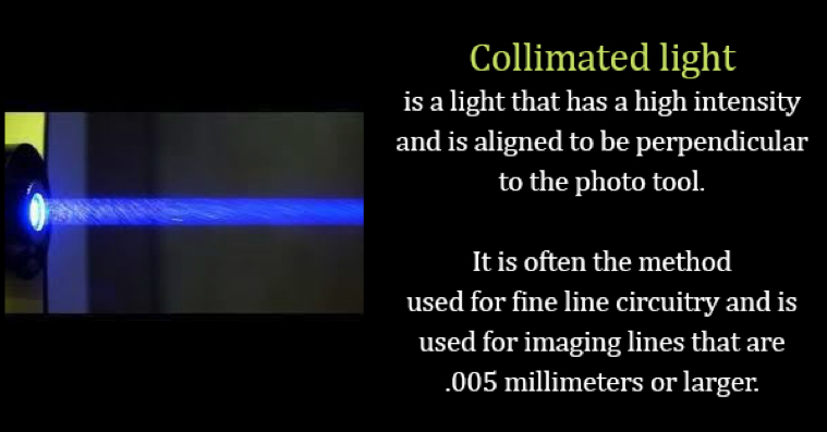
Collimated light
The photo tool that is used in LDI involves high-intensity UV light. This light will create a chemical reaction in the resist, which will cause it to harden. These UV sources are split into type types: non-collimated and collimated.
Collimated
Collimated light is a light that has a high intensity and is aligned to be perpendicular to the photo tool. It is often the method used for fine line circuitry and is used for imaging lines that are .005 millimeters or larger.
Non-collimated
This is a light that is not perpendicular to the board because it originates from a singular point. This means the light transmits at angles to the photo compared to the collimated light that comes directly from above. For this reason, this type of light is used for larger trace widths on prototype circuit boards.
If you are interested in learning more about laser direct imaging and how it can help you with your PCB assembly process, please don’t hesitate to contact our professionals today.